
We are still hand-drawing silicon?

The world is generating more signals than ever before, but the process of designing the circuitry that interprets those signals remains rather manual.
Analog and mixed-signal chips are the physical-to-digital translation layer of modern hardware. These chips are embedded in everything from the camera sensors guiding factory-floor robots and the LiDAR eyes of autonomous vehicles, to the tiny audio chips parsing voice commands for edge AI devices. They are the part of almost every chip that talks to the real world.
Yet, analog circuitry design remains one of the most manual parts of semiconductor engineering. Analog design cycles run slower, take more turns, carry more risk, and cost more than their digital counterparts. In modern mixed-signal chips, the analog section can account for less than 10% of the actual silicon area, yet it routinely consumes up to 90% of the total engineering effort and development time.
An error in these manual processes can be catastrophic. Imagine a wearable health company: if microscopic wires are drawn just a fraction of a hair too close together, it creates a physical electrical leak that permanently corrupts data, rendering a heart monitor unable to produce reliable readings. To fix it, the company must undergo a silicon respawn, a complete redesign and reprint of the physical chip, which can cost a startup millions and lead to months of product delays.
As demand for connected devices, robotics, autonomous systems, and edge AI accelerates, analog design complexity is increasing exponentially faster than human engineering productivity. This gap is the opportunity.
If a startup successfully automates analog design at scale, it has the potential to become a generational company (or be acquired by the big dogs). For reference, Synopsys and Cadence are the two publicly traded leaders that control ~85% of the digital electronic design automation (EDA) market with a combined market cap of $150B+ as of mid-2026, and both have been active on M&A to expand their capabilities into analog. Still, the problem isn't solved…
THE DIGITAL PLAYBOOK: A LADDER OF ABSTRACTION
Every chip is fundamentally an analog device, where transistors and voltages operate on a continuous spectrum. However, in digital chips, the continuous voltage signals produced by transistors are abstracted into 1s and 0s by setting voltage thresholds. Every gate acts as a firewall, taking noisy, imprecise physical signals and regenerating them into a clean 1 or 0. Imperfections accumulate locally but are reset at each stage, as long as the noise never crosses the voltage threshold, flipping the bit.
The digital chip industry and the entire EDA ecosystem has scaled successfully because of a ladder of abstraction. Over time, each new layer of abstraction pushed physics further into the background: transistors became switches, switches became logic gates, and logic gates eventually became code-like descriptions in Verilog or VHDL.
Crucially, this made chip design automatable. Once chip behavior could be described as code, software could translate it into physical reality, giving rise to the modern EDA industry, dominated by Synopsys, Cadence, and Siemens EDA, each built around key parts of that automation pipeline:
- Logic synthesis: turn code into logic gates.
- Place-and-route: turn logic gates into a chip layout.
- Verification: confirms that design behaves correctly (functional verification) and that the resulting layout will manufacture correctly (physical verification).
THE ANALOG REALITY: PHYSICS FIGHTS BACK
Analog integrated circuits resist clean abstraction. Unlike digital chips, there are no logic gates to constantly reset and clean the signal. The signal itself is the information, not just a carrier of a 1-or-0 decision. This means that every micro-interaction on the signal's journey matters continuously. Success in analog design requires absolute mastery over exact, continuous physical values, because once a value changes, that distortion carries forward.
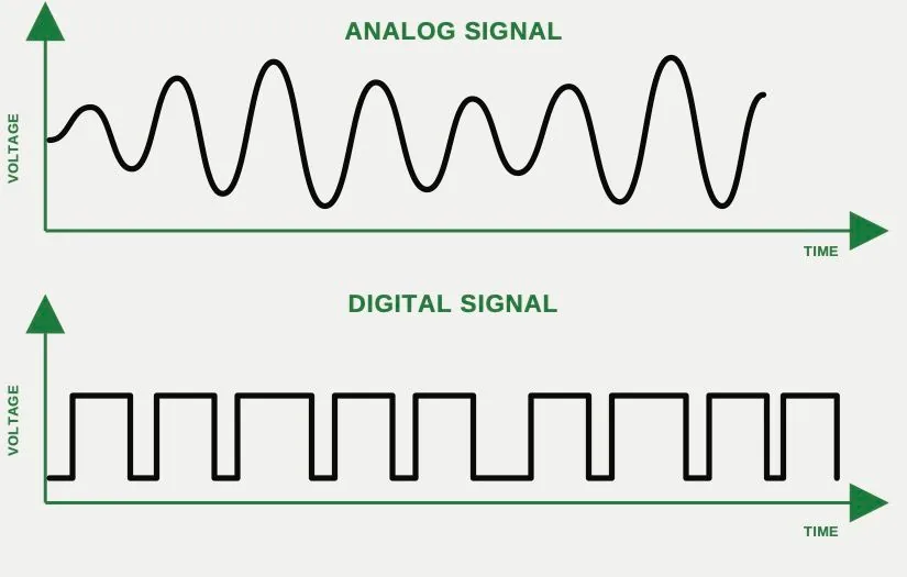
To look at a simplified, illustrative example of how this plays out across two transistors:
- If the circuit is digital with a threshold of 3V: The first transistor outputs 5V, which reads as a logical 1 because it exceeds the threshold. Noise along the wire reduces the signal to 4V. The second transistor still reads it as a logical 1 because it is above the 3V threshold, resets the signal, and outputs a clean 5V. The noise is removed.
- If the circuit is analog: The first transistor outputs 5V because it is measuring something specific, like an audio volume or a sensor reading. Noise reduces that signal to 4V. Since analog allows every voltage to be a valid measurement (continuous spectrum), the next stage has no reference point to know that 4V is an error, so it treats it as an intentional truth from the real world, amplifies it, and passes it on. Without a threshold, the transistor has no boundary line to tell it what is noise and what is data, so the noise can have an impact on the final output, altering the measurement.
This means analog designers can’t ignore the underlying physics. They have to account for an overwhelming number of physical variables that digital designers get to abstract away. They have to account for parasitic effects (unintended capacitance, resistance, and cross-talk) that constantly distort the signals, meaning the physical layout of the chip fundamentally changes how the chip behaves.
Because of this, traditional analog design has remained an artisanal, manual process, heavily reliant on human intuition and SPICE simulations.
Developing design and simulation tools to automate this workflow is the current challenge for the EDA industry, and there are generally two camps in analog design automation:
(1) Bottom-Up: build fundamental building blocks enabling abstraction.
For decades, academia and early EDA startups tried to automate analog design using the digital playbook: building reusable, abstracted blocks like logic gates. However, as Moore’s Law advanced (the observation that the number of transistors on a silicon chip will double every two years with minimal rise in cost), manufacturing advances and inconsistencies kept changing transistor behavior, rendering past abstractions obsolete with every new process node.
While the goal is no longer to abstract the transistor, there are other building blocks. Instead of focusing on individual components, modern designers are moving up the stack toward higher-level reusable pieces.
(2) Top-Down: treat the circuit as a math problem by specifying intent and automating the execution.
Top-down abandons the idea of pre-made building blocks entirely, accepting that analog physics is inherently noisy. Using artificial intelligence (AI), machine learning (ML), and brute-force simulation, these tools test thousands of designs at once, searching for one that meets spec rather than assembling one from trusted parts.
This approach has also been attempted for decades and can suffer from a verification gap: finding a design that meets specs in nominal simulation is very different from proving that design holds up across real-world process, voltage, and temperature (PVT) variation.
That said, advances in AI/ML have reignited interest in the top-down approach.
THE OPPORTUNITY
As edge AI, robotics, and smart sensors explode, the industry can no longer afford to hand-draw the future of silicon. This manual analog design process is holding back the hardware industry and the tools that fix this bottleneck will unlock the next era of silicon productivity.
If you're a founder building in this space, navigating the verification gap, or designing the next generation of analog EDA software, we would love to connect.